New record of electron diffraction
Materials science researchers in the UK and Germany have developed a new electron microscopy technique that enables the creation of electron diffraction images from a material area with a radius of only 10 nm with a major degree. The body has never been seen before.
This method also allows the size of the diffraction zone to be carefully adjusted to the desired properties in each material in particular, allowing for the first time the influence of the excluded material to be excluded. (According to new results published in Applied Physics Letters ).
Transmission Electron Microscope (TEM) can produce electron diffraction images of nanometer-sized samples, and is an extremely effective method for analyzing nanometer materials. . In these diffraction experiments, scientists can use both methods as convergent electron beam electron diffraction (with focused electron beam) or regionally selected electron diffraction with electron beam parallel. Each way has its advantages and disadvantages, the conventional parallel beam beam is easy to use and simpler, easy for the defined diffraction spectrum.

Figure 1. Improved optical diagram on JEM-2200FS device
at Oxford University ( Appl. Phys. Lett. 90, 151104 ).
However, due to the limitations of the working range of the objective lens used in electron microscopes, such electron beams are difficult to converge at a small size point. For this reason, most experiments conducted with parallel electron beams are often used in a mode called out-of-focus (meaning that beyond the convergence point), and can produce many effects. undesirable (eg Fresnel striae) and it is difficult to select a small diffraction volume area that allows analysis with parallel electron beams.
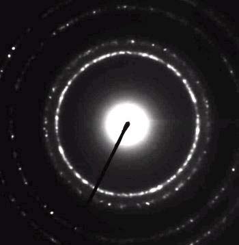
Recently, the group of Christian Dwyer and colleagues at Oxford University (UK) and colleagues at CEOS GmbH (Heidelberg, Germany) have shown that it is possible to create converged parallel beams of electrons. in a sharp way to eliminate the problems mentioned above. The researchers conducted by exploiting the complementary sunng lenses that were added to the microscope at Oxford University to achieve the optimal upper and lower diverging beam levels for transmitting microscopes. system. Using this technique, the team achieved the technique of electron beam diffraction parallel to the selected area for diffraction with a diameter as small as 10 nm, with an accuracy of up to 0.5 nm.
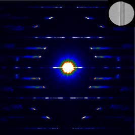
Figure 2. Results of electron diffraction spectra select 10 nm region
on multi-walled tungsten nanotubes disulphide (Appl. Phys. Lett. 90, 151104).
"The advantage of this method is to achieve very high precision with very small diffraction areas, very flexible with selected materials" - Dwyer said on Nanotechweb.org - "Therefore, experimentalists can choose correctly select the area of the material you want to analyze and can be confident that the surrounding area will not affect this analysis. "
The collaborative research group between the UK and Germany will seek out the advantages and disadvantages of this method to be able to exploit electron diffraction techniques."This indirect method can give us information about the crystal structure of the material at a good resolution, much smaller than the ability of traditional electron microscopy techniques" - in words. by Dwyer.
SAED easy to implement but difficult to implement on a small area?
The Doctrine of Independence
According to Belle Dumé - NanotechWeb.org, Vietnamese Physics
- New Zealand: Successfully tested the Electron boosters
- LHC broke the world record for energy generation
- Detection of bacteria 'eat' electrons
- The world goes through an electron microscope
- Manufacturing small components under 10 nm by electron microscopy
- Capture tiny objects with a new generation microscope
- Successful data transfer by laboratory teleport technology
- Spintronic memory breakthrough
- Use quantum dots as a single electron emission source at will
- Great invention: Found legendary nuts
- Why does the microscope output monochrome images?
- 32 people set themselves on fire to set a world record
 Special weight loss device helps prevent appetite
 Daily use inventions come from universities
 8 inventors were killed by their own inventions
 Iran invented a motor car powered by water